IBM beats optical lithography limits
IBM develops an optical lithography technique capable of producing structures less than 32 nm in size which its says gives the industry seven years of breathing space.
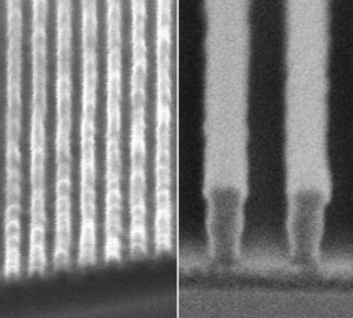
Scientists at IBM say they have fabricated distinct and uniformly spaced ridges only 29.9 nm wide using 193-nm lithography. This beats the 32 nm mark that industry had held as the limit for optical lithography. The result potentially postpones the semiconductor industry's conversion to alternatives such as extreme ultraviolet lithography.
"Our goal is to push optical lithography as far as we can so the industry does not have to move to any expensive alternatives until absolutely necessary," said Robert Allen, manager of lithography materials at IBM's Almaden Research Center. "This result is the strongest evidence to date that the industry may have at least seven years of breathing room before any radical changes in chip-making techniques would be needed."
The pattern of well-defined and equally spaced 29.9-nanometer lines and spaces was created on a lithography test apparatus designed and built at IBM Almaden, using new materials developed by its collaborator, JSR Micro of Sunnyvale, California. The first technical details will be presented at this week's microlithography conference being held in San Jose, California, US.
The wavelength used for lithography has steadily come down to 193 nm, which is the current basis for chip manufacturing. Until now, it was not known if the industry could continue to adapt optical immersion techniques, which involves adding a liquid between the lens and the water, to fabricate smaller feature sizes.
"We believe that high-index liquid imaging will enable the extension of today's optical lithography through the 45- and 32-nanometer nodes," said Mark Slezak, technical manager of JSR Micro. "Our industry faces tough questions about which lithography technology will allow us to be successful below 32 nanometers. This result gives us another data point favouring the continuation of optical immersion lithography."
To fabricate the pattern, IBM developed an interference immersion lithography set-up which it calls NEMO. IBM's NEMO tool uses two intersecting laser beams to create interference patterns with spacings closer than can be produced with current chip-making apparatus.
As a result, NEMO is ideal for researching, testing and optimizing various high-index fluids and photoresists being considered for use in future 193 nm systems. Now that IBM's result shows a path for extending optical lithography, high-index lens materials must be developed to enable its commercial viability.
Resolution in immersion lithography is limited by the lowest refractive index of the final lens, fluid and photoresist materials. Light passing through a higher-index material has a shorter wavelength and can thus be focused more tightly.
In IBM's NEMO experiments, the lens and fluid had indices of refraction of around 1.6, and the photoresist's index of refraction was 1.7. Research is now ongoing to develop lens, fluid and photoresist materials with indices of refraction of 1.9, which would enable even smaller features to be written.
